GRAD Engineering LLC
|
GRAD Engineering LLC |
|
Programmable
Logic Device and Programmable Logic Array are terms for integrated circuits that
can be programmed to perform complex functions. A design is programmed into the device by blowing hundreds of
micro fuses. I
assume the reader knows an AND gate from an OR gate. Here we will talk about programmable logic ICs.
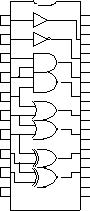
The IC below includes eight different logic functions.
To use TTL logic this will take an 74LS08 AND gate, 74LS04 Inverter,
74LS02 NOR gate….etc. Using programmable logic we can push all this logic into
one IC. The designer can greatly
reduce the printed circuit real estate used. A
design change may take only minutes. No
soldering iron needed.
The
best part of programmable logic is “its programmability”.
To make this IC I typed this into my computer.
Thirty seconds later I had a custom IC. PIN
19 = PIN 1 PIN
18 = /PIN 2 PIN
17 = PIN 3 * PIN 4 /PIN
16 = PIN 4 * PIN 5 PIN
15 = PIN 5 + PIN 6 /PIN
14 = PIN 6 + PIN 7 PIN
13 = PIN 7 :+: PIN 8 /PIN
12 = PIN 8 :+: PIN 9 The
input of the inverter can be any input pin, just as the output can be on any
output pin. This greatly eases the
printed circuit board layout. To
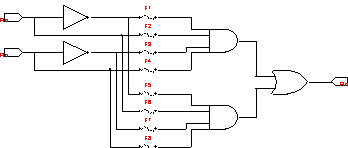
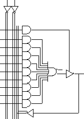
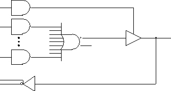
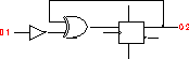
understand programmable logic arrays look at a simplified schematic of a
PLD. Signal from the two input pins
and the inverse of these signal are fed into a bank of fuses F1 through F8.
The AND gates are OR-ed together which drives the output pin.
By
blowing open certain fuses all many gate combinations can be programmed into
this simple PAL.
This
design is based around a PAL10H8 which is not in production now.
You can see the data sheet at my web site.
It is much like my simple schematic but with 10 input pins and 8 output
pins. Each AND gate has 20 inputs
or 20 fuses. Why 20 fuses?
There are 10 inputs and the inverse of those inputs.
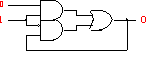
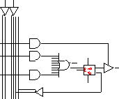
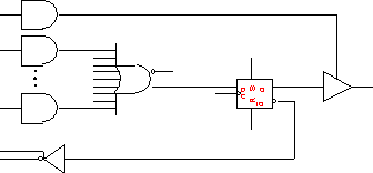
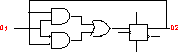
LATCH
A simple latch can be made.
When L is high data flows from D to Q.
When L in low the data on Q is held independent of the D input.
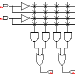
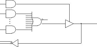
AND OR Combination CellSchematics
of the inside of a PAL are drawn like this.
Each “X” is a fuse and a diode.
This method is much simpler than drawing each fuse.
See
10H8
I/O Cell A
pin can be set to input, output or dynamically programmed as I/O.
The fuse block is far larger than shown here.
All AND gates can connect to all of the ten inputs and all of the I/O
pins.
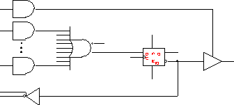
See 16L8 Registered Cell A registered cell consists of a D-flip flop at the output of AND OR combinational logic. This cell is used to make state machines, counters and shift registers.
See
16R8 PAL Many
things have changed cense the first programmable logic device.
Fuses have been replaced with flash memory allowing easy erasure and
reprogramming. There used to be
hundreds (more or less) of different kinds of PLD.
The industry moved to parts like the 16V8 and 22V10 which can replace
almost all of the older parts. Programmable
Array Logic is basically more of the same but bigger and more flexible.
To get a data sheet for the 22V10 go to digikey.com and search for 22V10.
Then down load the PDF file.
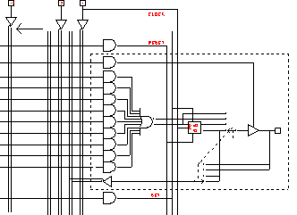
Simplified
schematic of a 22V10 PLD There
are 12 input pins and 10 I/O pins. The
dotted box is repeated ten times. Each
AND gate has 44 inputs. Every
input, it’s inverse and every I/O pin and it’s inverse are fed into the fuse
block. The bank of fuses total
roughly 6,000. The
D flip flops have a common rising edge clock, asynchronous reset and
asynchronous set controls. Each
input/output pin has a tri-state buffer controlled by one AND gate.
Each logic block is individually programmed to use/not use the flip flop.
There are four options selected by two fuses.
Option
one is a simple AND OR array with tri-state buffer. The pin can be fixed as input or fixed as output, dynamically
set as input or output. To be
pin-out compatible with older parts I used the inverse of Pin 11 to drive some
or all of the tri-state controls. The
I/O pin is fed back into the fuse block.
The
second option is AND NOR array.
Option
3 uses a D- flip flop. Data
on D is latched on the rising edge of Pin 1 (clock).
Note the feedback now is from the FF and not the I/O pin.
Option
4 inverts the output but not the feedback. Program I
use my EPROM programmer to program PLDs. In
programming mode a PLD looks like a small EPROM or FLASH memory.
In the case of the 22V10 the first 44 locations in memory are the 44
fuses for the first AND gate. Each
AND gate uses the next 44 fuses. Location
0 connects Pin1 while location 1 connects 1/Pin1.
Location 4 and 5 connects Pin2 and 1/Pin2. Software: I
have used PALASM, ABEL and CUPL. A
quick search of the Internet shows that several universities are still using
PALASM. There are sites for the
students to down the software and tutorials.
A DOS PLD development program is not exciting but the price is right!
I have put PALASM on my web site, see the end of the article.
Learn by example: PATTERN
A REVISION
3.0 AUTHOR
J.ENGINEER COMPANY
ADVANCED MICRO DEVICES DATE
10/01/04 CHIP
DECODER PAL16L8 ;----------
PIN Declarations ----- PIN
1 CLK
COMBINATORIAL ; INPUT PIN
2 X
COMBINATORIAL ; INPUT PIN
3 Y
COMBINATORIAL ; INPUT PIN
4 Z
COMBINATORIAL ; INPUT PIN
5 GO
COMBINATORIAL ; INPUT PIN
6 STOP COMBINATORIAL ; INPUT PIN
10 GND
; INPUT PIN
12 A COMBINATORIAL
; OUTPUT PIN
13 B COMBINATORIAL
; OUTPUT PIN
14 C COMBINATORIAL
; OUTPUT PIN
15 D COMBINATORIAL
; OUTPUT PIN
16 E COMBINATORIAL
; OUTPUT PIN
17 F COMBINATORIAL
; OUTPUT PIN
18 G COMBINATORIAL
; OUTPUT PIN
19 H COMBINATORIAL
; OUTPUT PIN
20 VCC
; INPUT EQUATIONS /A
= /X * /Y * /Z A.TRST
= GO * /STOP /B
= /X * /Y * Z B.TRST
= GO * /STOP /C
= /X * Y * /Z C.TRST
= GO * /STOP /D
= /X * Y *
Z D.TRST
= GO * /STOP /E
= X * /Y * /Z E.TRST
= GO * /STOP /F
= X * /Y *
Z F.TRST
= GO * /STOP /G
= X *
Y * /Z G.TRST
= GO * /STOP /H
= X *
Y * Z H.TRST
= GO * /STOP Most
software have the same requirements. Define
what type of IC. PAL16L8 Define
PINs as to input, output or IO.
Give PINs names. (optional) Define
EQUATIONS.
/H = X and Y and Z 3 input NAND gate Counter EQUATIONS ;EIGHT
BIT COUNTER Q1:=/Q1
;
OUT=1/Q1 Q2:=(Q2
:+: /Q1)
;
Q3:=(Q3
:+: (/Q2*/Q1)) Q4:=(Q4
:+: (/Q3*/Q2*/Q1)) Q5:=(Q5
:+: (/Q4*/Q3*/A2*/Q1)) Q6:=(Q6
:+: (/Q5*/Q4*/Q3*/A2*/Q1)) Q7:=(Q7
:+: (/Q6*/Q5*/Q4*/Q3*/A2*/Q1)) Q8:=(Q8
:+: (/Q7*/Q6*/Q5*/Q4*/Q3*/A2*/Q1))
The
equation Q1:= causes a flip flop to be used.
The D input of the flip flop is the inverse of the Q output.
This will cause the output to change every clock.
Q2:
toggles when Q1=0. This will cause
the output to change every other clock.
Q3:
holds it’s present value when D1 and D2 is not 00. When D1,2 is 00 then Q3 changes state. What Really Happened A
22V10 does not have an XOR function. So
what really happened! I looked at
the fuse map and found this.
If
Q1=1 then the FF will hold. If Q1=0
then the FF will toggle. This is a
T flip flop. Output file The
software takes equations like /H=X*Y*Z and produces program files like this.
Each “0” or “1” represents a fuse open or closed.
In this case each line is for one AND gate. L0000
01111111111111111111111111111111* L0032
11111111111111111111111111111101* L0064
00000000000000000000000000000000* L0096
00000000000000000000000000000000* L0128
00000000000000000000000000000000* L0160
00000000000000000000000000000000* L0192
00000000000000000000000000000000* L0224
00000000000000000000000000000000* L0256
11111111111111111111111111111101* L0288
11110111111111111111111111111111* L0320
11111111111111111111111101111111* L0352
11111111111111111111111111110111* Partial
listing for a PAL16V8. CPLDVery
quickly: A CPLD is a Complex
Programmable Logic Device. Basically
a CPLD is four to ten 22V10s in one package.
Here we are talking about 100s of logic elements.
See
MAX 3000 and MAX 5000 Next Month FPGA Next
month, FPGAs with 100,000 logic elements, memory and a CPU!
This is where the big boys play! About the Author Ron
Simpson is attending the university of hard knocks. His designs have been produced by over thirty companies. You
may reach him at ron@gradllc.com.
More information can be found at www.gradllc.com
go to white papers then to PLD. About the Author
DownLoad:DownLoads/WinNT.html |
|
|